
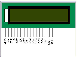
LCD (16 by 2):-
LCD (Liquid Crystal Display) screen is an electronic display module
and find a wide range of applications. A 16x2 LCD display is very basic
module and is very commonly used in various devices and circuits.
These modules are preferred over seven and other multi segment Leds.
The reasons being: LCDs are economical; easily programmable; have no
limitation of displaying special & even custom characters
(unlike in seven segments), animations and so on.
A 16x2 LCD means it can display 16 characters per line and there are 2
such lines. In this LCD each character is displayed in 5x7 pixel
matrix. This LCD has two registers, namely, Command and Data.
The
command register stores the command instructions given to the LCD. A
command is an instruction given to LCD to do a predefined task like
initializing it, clearing its screen, setting the cursor position,
controlling display etc. The data register stores the data to be
displayed on the LCD. The data is the ASCII value of the character to be
displayed on the LCD.
Transmission through RF is better than IR (infrared) because of many reasons. Firstly, signals through RF can travel through larger distances making it suitable for long range applications. Also, while IR mostly operates in line-of-sight mode, RF signals can travel even when there is an obstruction between transmitter & receiver. Next, RF transmission is more strong and reliable than IR transmission. RF communication uses a specific frequency unlike IR signals which are affected by other IR emitting sources.


ADC0804 is a very commonly used 8-bit analog to digital convertor. It is a single channel IC, i.e., it can take only one analog signal as input. The digital outputs vary from 0 to a maximum of 255. The step size can be adjusted by setting the reference voltage at pin9. When this pin is not connected, the default reference voltage is the operating voltage, i.e., Vcc. The step size at 5V is 19.53mV (5V/255), i.e., for every 19.53mV rise in the analog input, the output varies by 1 unit. To set a particular voltage level as the reference value, this pin is connected to half the voltage. For example, to set a reference of 4V (Vref), pin9 is connected to 2V (Vref/2), thereby reducing the step size to 15.62mV (4V/255).
ADC0804 needs a clock to operate. The time taken to convert the analog value to digital value is dependent on this clock source. An external clock can be given at the Clock IN pin. ADC 0804 also has an inbuilt clock which can be used in absence of external clock. A suitable RC circuit is connected between the Clock IN and Clock R pins to use the internal clock.


Pin Description:
Pin No
|
Function
|
Name
|
1
|
Ground (0V)
|
Ground
|
2
|
Supply voltage; 5V (4.7V – 5.3V)
|
Vcc
|
3
|
Contrast adjustment; through a variable resistor
|
VEE
|
4
|
Selects command register when low; and data register when high
|
Register Select
|
5
|
Low to write to the register; High to read from the register
|
Read/write
|
6
|
Sends data to data pins when a high to low pulse is given
|
Enable
|
7
|
8-bit data pins
|
DB0
|
8
|
DB1
| |
9
|
DB2
| |
10
|
DB3
| |
11
|
DB4
| |
12
|
DB5
| |
13
|
DB6
| |
14
|
DB7
| |
15
|
Back light VCC (5V)
|
Led+
|
16
|
Backlight Ground (0V)
|
Led-
|
RF MODULE:-
The
RF module, as the name suggests, operates at Radio Frequency. The
corresponding frequency range varies between 30 kHz & 300 GHz. In
this RF system, the digital data is represented as variations in the
amplitude of carrier wave. This kind of modulation is known as Amplitude
Shift Keying (ASK). Transmission through RF is better than IR (infrared) because of many reasons. Firstly, signals through RF can travel through larger distances making it suitable for long range applications. Also, while IR mostly operates in line-of-sight mode, RF signals can travel even when there is an obstruction between transmitter & receiver. Next, RF transmission is more strong and reliable than IR transmission. RF communication uses a specific frequency unlike IR signals which are affected by other IR emitting sources.
This RF module comprises of an RF Transmitter and an RF Receiver. The transmitter/receiver (Tx/Rx) pair operates at a frequency of 434 MHz.
An RF transmitter receives serial data and transmits it wirelessly
through RF through its antenna connected at pin4. The transmission
occurs at the rate of 1Kbps - 10Kbps.The transmitted data is received by
an RF receiver operating at the same frequency as that of the
transmitter.
The
RF module is often used alongwith a pair of encoder/decoder. The
encoder is used for encoding parallel data for transmission feed while
reception is decoded by a decoder. HT12E-HT12D, HT640-HT648, etc. are some commonly used encoder/decoder pair ICs.

Pin Description:
RF Transmitter
Pin No
|
Function
|
Name
|
1
|
Ground (0V)
|
Ground
|
2
|
Serial data input pin
|
Data
|
3
|
Supply voltage; 5V
|
Vcc
|
4
|
Antenna output pin
|
ANT
|
RF Receiver
Pin No
|
Function
|
Name
|
1
|
Ground (0V)
|
Ground
|
2
|
Serial data output pin
|
Data
|
3
|
Linear output pin; not connected
|
NC
|
4
|
Supply voltage; 5V
|
Vcc
|
5
|
Supply voltage; 5V
|
Vcc
|
6
|
Ground (0V)
|
Ground
|
7
|
Ground (0V)
|
Ground
|
8
|
Antenna input pin
|
ANT
|
7 SEGMENT DISPLAY
A
seven segment display is the most basic electronic display device that
can display digits from 0-9. They find wide application in devices that
display numeric information like digital clocks, radio, microwave ovens,
electronic meters etc. The most common configuration has an array of
eight LEDs arranged in a special pattern to display these digits. They are laid out as a squared-off figure ‘8’.
Every LED is assigned a name from 'a' to 'h' and is identified by its
name. Seven LEDs 'a' to 'g' are used to display the numerals while
eighth LED 'h' is used to display the dot/decimal.
A
seven segment is generally available in ten pin package. While eight
pins correspond to the eight LEDs, the remaining two pins (at middle)
are common and internally shorted. These segments come in two
configurations, namely, Common cathode (CC) and Common anode (CA). In CC
configuration, the negative terminals of all LEDs are connected to the
common pins. The common is connected to ground and a particular LED
glows when its corresponding pin is given high. In CA arrangement, the
common pin is given a high logic and the LED pins are given low to
display a number.
PIN DIAGRAM:-

ADC 0804:-
Analog
to digital converters find huge application as an intermediate device
to convert the signals from analog to digital form. These digital
signals are used for further processing by the digital processors.
Various sensors like temperature, pressure, force etc. convert the
physical characteristics into electrical signals that are analog in
nature.
ADC0804 is a very commonly used 8-bit analog to digital convertor. It is a single channel IC, i.e., it can take only one analog signal as input. The digital outputs vary from 0 to a maximum of 255. The step size can be adjusted by setting the reference voltage at pin9. When this pin is not connected, the default reference voltage is the operating voltage, i.e., Vcc. The step size at 5V is 19.53mV (5V/255), i.e., for every 19.53mV rise in the analog input, the output varies by 1 unit. To set a particular voltage level as the reference value, this pin is connected to half the voltage. For example, to set a reference of 4V (Vref), pin9 is connected to 2V (Vref/2), thereby reducing the step size to 15.62mV (4V/255).
ADC0804 needs a clock to operate. The time taken to convert the analog value to digital value is dependent on this clock source. An external clock can be given at the Clock IN pin. ADC 0804 also has an inbuilt clock which can be used in absence of external clock. A suitable RC circuit is connected between the Clock IN and Clock R pins to use the internal clock.

Pin Description:
Pin No
|
Function
|
Name
|
1
|
Activates ADC; Active low
|
Chip select
|
2
|
Input pin; High to low pulse brings the data from internal registers to the output pins after conversion
|
Read
|
3
|
Input pin; Low to high pulse is given to start the conversion
|
Write
|
4
|
Clock Input pin; to give external clock.
|
Clock IN
|
5
|
Output pin; Goes low when conversion is complete
|
Interrupt
|
6
|
Analog non-inverting input
|
Vin(+)
|
7
|
Analog inverting Input; normally ground
|
Vin(-)
|
8
|
Ground(0V)
|
Analog Ground
|
9
|
Input pin; sets the reference voltage for analog input
|
Vref/2
|
10
|
Ground(0V)
|
Digital Ground
|
11
|
8 bit digital output pins
|
D7
|
12
|
D6
| |
13
|
D5
| |
14
|
D4
| |
15
|
D3
| |
16
|
D2
| |
17
|
D1
| |
18
|
D0
| |
19
|
Used with Clock IN pin when internal clock source is used
|
Clock R
|
20
|
Supply voltage; 5V
|
Vcc
|
ULN2003:-
ULN2003
is a high voltage and high current Darlington array IC. It contains
seven open collector darlington pairs with common emitters. A darlington
pair is an arrangement of two bipolar transistors.
ULN2003
belongs to the family of ULN200X series of ICs. Different versions of
this family interface to different logic families. ULN2003 is for 5V
TTL, CMOS logic devices. These ICs are used when driving a wide range of
loads and are used as relay drivers, display drivers, line drivers etc.
ULN2003 is also commonly used while driving Stepper Motors. Refer Stepper Motor interfacing using ULN2003.
Each
channel or darlington pair in ULN2003 is rated at 500mA and can
withstand peak current of 600mA. The inputs and outputs are provided
opposite to each other in the pin layout. Each driver also contains a
suppression diode to dissipate voltage spikes while driving inductive
loads. The schematic for each driver is given below:

Pin Description:
Pin No
|
Function
|
Name
|
1
|
Input for 1st channel
|
Input 1
|
2
|
Input for 2nd channel
|
Input 2
|
3
|
Input for 3rd channel
|
Input 3
|
4
|
Input for 4th channel
|
Input 4
|
5
|
Input for 5th channel
|
Input 5
|
6
|
Input for 6th channel
|
Input 6
|
7
|
Input for 7th channel
|
Input 7
|
8
|
Ground (0V)
|
Ground
|
9
|
Common free wheeling diodes
|
Common
|
10
|
Output for 7th channel
|
Output 7
|
11
|
Output for 6th channel
|
Output 6
|
12
|
Output for 5th channel
|
Output 5
|
13
|
Output for 4th channel
|
Output 4
|
14
|
Output for 3rd channel
|
Output 3
|
15
|
Output for 2nd channel
|
Output 2
|
16
|
Output for 1st channel
|
Output 1
|
EEPROM:-
AT24C02
is an electrically erasable and programmable ROM. It has a 2Kbits of
memory size arranged in 32 pages of 8 byte each. There are 256 (32 x 8)
words each of one byte. The data is transferred and received serially
through serial data (SDA) pin.
The SCL is clock input and is used to synchronize EEPROM with microcontroller
for various operations. When data is to be read or write, first a start
condition is created followed by device address, byte address and the
data itself. Finally a stop condition is provided. The start condition
occurs when SDA and SCL get high to low simultaneously. The stop
condition is when SDA remains low while SCL goes from high to low. The
data is read or written between the start and stop conditions on every
transition of SCL from high to low. For more details on different
operations and addressing, refer interfacing 24C02 with 8051.
A
total of eight EEPROMs can be connected through a bus. There are three
address pins in AT24C02 for selecting a particular chip. The device can
be addressed serially by the software. It makes use of an internal
register of the EEPROM whose 4 MSB bits are 1010, the next three are the
EEPROM address bits and the LSB signifies whether data is to be read or
written. This last bit is 1 for write and 0 for read operation.
For
example, if in an EEPROM all address bits are grounded, then for write
operation a hex value 0xA1 (1010 0001) will be sent. Here 000, in last
bits, addresses the EEPROM and 1 in LSB indicates a write operation.
Similarly for read operation the device address to be sent is 0xA0 (1010
0000).
Next,
the byte or page address is sent followed by the data byte. This data
byte is to be written on or read by the microcontroller.
Pin Diagram:

Pin Description:
Pin No
|
Function
|
Name
|
1
|
Address input pins; Provide addresses when more than one EEPROM is interfaced to a single microcontroller;
Ground when only one EEPROM is used
|
AD0
|
2
|
AD1
| |
3
|
AD2
| |
4
|
Ground (0V)
|
Ground
|
5
|
Bi-directional pin for serial data transfer
|
Serial Data
|
6
|
Provides clock signals
|
Serial Clock
|
7
|
Ground allows normal read/write functions;
Vcc enables write protection
|
Write protect
|
8
|
Supply voltage; 5V (up to 5.5V)
|
Vcc
|
MAX232:-
The
MAX232 IC is used to convert the TTL/CMOS logic levels to RS232 logic
levels during serial communication of microcontrollers with PC. The
controller operates at TTL logic level (0-5V) whereas the serial
communication in PC works on RS232 standards (-25 V to + 25V). This
makes it difficult to establish a direct link between them to
communicate with each other.
The intermediate link is provided through MAX232. It is
a dual driver/receiver that includes a capacitive voltage generator to
supply RS232 voltage levels from a single 5V supply. Each receiver
converts RS232 inputs to 5V TTL/CMOS levels. These receivers (R1 & R2) can accept ±30V inputs. The drivers (T1 & T2), also called transmitters, convert the TTL/CMOS input level into RS232 level.
The
transmitters take input from controller’s serial transmission pin and
send the output to RS232’s receiver. The receivers, on the other hand,
take input from transmission pin of RS232 serial port and give serial
output to microcontroller’s receiver pin. MAX232 needs four external capacitors whose value ranges from 1µF to 22µF.
Microcontroller
|
MAX232
|
RS232
| |
Tx
|
T1/2 In
|
T1/2 Out
|
Rx
|
Rx
|
R1/2 Out
|
R1/2 In
|
Tx
|
Pin Diagram:

Pin Description:
Pin No
|
Function
|
Name
|
1
|
Capacitor connection pins
|
Capacitor 1 +
|
2
|
Capacitor 3 +
| |
3
|
Capacitor 1 -
| |
4
|
Capacitor 2 +
| |
5
|
Capacitor 2 -
| |
6
|
Capacitor 4 -
| |
7
|
Output pin; outputs the serially transmitted data at RS232 logic level; connected to receiver pin of PC serial port
|
T2 Out
|
8
|
Input pin; receives serially transmitted data at RS 232 logic level; connected to transmitter pin of PC serial port
|
R2 In
|
9
|
Output pin; outputs the serially transmitted data at TTL logic level; connected to receiver pin of controller.
|
R2 Out
|
10
|
Input pins; receive the serial data at TTL logic level; connected to serial transmitter pin of controller.
|
T2 In
|
11
|
T1 In
| |
12
|
Output pin; outputs the serially transmitted data at TTL logic level; connected to receiver pin of controller.
|
R1 Out
|
13
|
Input pin; receives serially transmitted data at RS 232 logic level; connected to transmitter pin of PC serial port
|
R1 In
|
14
|
Output pin; outputs the serially transmitted data at RS232 logic level; connected to receiver pin of PC serial port
|
T1 Out
|
15
|
Ground (0V)
|
Ground
|
16
|
Supply voltage; 5V (4.5V – 5.5V)
|
Vcc
|
No comments:
Post a Comment